

Several reasons for poor soldering on the tin surface of circuit boards
circuit board manufacturerWe have summarized several viewpoints on poor soldering on the tin surface of circuit boards, which we can refer to and hope can be helpful to us. The main factors that contribute to poor soldering of PCB boards are from two aspects: circuit board manufacturers and surface mount manufacturers
1. Storage environment and transportation: This is the link between the PCB manufacturer and the SMT factory. Generally, PCBs are rarely in stock, but general inventory requires a suitable storage environment with appropriate dryness and humidity, intact packaging, and should be handled gently during transportation. Vacuum packaging damage should not be allowed to be stored for a long time. The theoretical storage time for tinplate is one month, but the best soldering time is within 48 hours. If the storage time exceeds one month, it is recommended to return to the PCB factory and use special solution to sort and bake the board. Baking board parameters 150 ° for 1 hour
2. The operation during shipment did not follow the operating standards: The circuit profession has extremely strict requirements for the workshop environment and the standard operation of employees, especially in the production process of circuit boards, which requires a chemical reaction environment. Therefore, impurities are not allowed to enter. After the tin spraying process of the board is completed, a series of subsequent operations require employees to wear anti-static gloves. Due to finger sweat or stains directly touching the surface, it will form surface oxidation. If it forms a defect, it is extremely difficult to detect, and it is presented irregularly. Testing and tin plating experiments are difficult to expose.
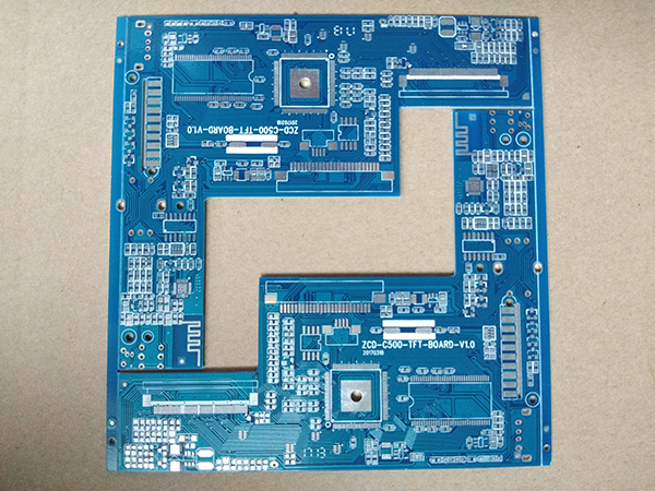
3. Welding disadvantages caused by warping: During the welding process, circuit boards and components may warp, leading to defects such as virtual soldering and short circuits due to stress deformation. Warping is often caused by temperature imbalance between the upper and lower parts of the circuit board. Large PCBs can also warp due to the weight of the board itself falling. The distance between ordinary PBGA equipment and printed circuit boards is about 0.5mm. If the equipment on the circuit board is large, as the circuit board cools down and returns to its normal shape, the solder joints will be under stress for a long time. If the equipment is raised by 0.1mm, it is enough to cause virtual soldering and open circuit. For special products, it is required that the PCB factory use yin-yang splicing to reduce warping, and perhaps adopt a splicing board of appropriate size as much as possible, without being too large or too small.
4. The issue of tin source for incoming materials: Regarding material procurement, some circuit board factories blindly pursue cost cutting. When using tin sprayed raw tin, they purchase recycled tin from professional sources, which may have unstable content. Generally, circuit board factories with extremely low unit prices may have such a dangerous probability. It is recommended that we carefully choose suppliers.
5. Failure to timely remove slag and tidy up the tin furnace used for tin spraying: Timely maintenance of the tin furnace is very important. As tin spraying is a vertical cycle process, the circuit board surface will be under strong pressure. For those boards with incomplete solder mask and weak characters, impact will occur, causing them to fall off and deposit in the furnace. Through high temperature evaporation, if left untreated for too long, it will form external adhesion.
Article sourced from Jiangmen single and double-sided circuit boardhttp://www.yonghongpcb.com
-
09-09
Schematic diagram of Jiangmen single and double-sided circuit board
1. There are now various specialized PCB drawing software, such as Protel, which can draw multi-layer (including double-sided) circuit board diagrams. The layers are aligned in orientation and have vi
-
09-09
Schematic diagram of Jiangmen single and double-sided circuit board
1. There are now various specialized PCB drawing software, such as Protel, which can draw multi-layer (including double-sided) circuit board diagrams. The layers are aligned in orientation and have vi
-
09-09
Schematic diagram of Jiangmen single and double-sided circuit board
1. There are now various specialized PCB drawing software, such as Protel, which can draw multi-layer (including double-sided) circuit board diagrams. The layers are aligned in orientation and have vi
-
04-27
What is the structure of blind buried hole circuit board?
blind and buried viascircuit boardIt has the ability to freely bend, fold, and roll, and can move and stretch freely in three-dimensional space; Good heat dissipation performance and high precision; T