

What is the structure of blind buried hole circuit board?
blind and buried viascircuit boardIt has the ability to freely bend, fold, and roll, and can move and stretch freely in three-dimensional space; Good heat dissipation performance and high precision; To achieve features such as lightweighting, miniaturization, and thinning, and to achieve integration of component devices and wire connections, let's take a look at its structure and exterior treatment together.
structure
Blind buried hole circuit boards mainly include blind holes and buried holes. Blind holes refer to the outer surfaces of the top and bottom layers of printed circuit boards, with a certain depth, used for connecting surface circuits and inner layer circuits below. The depth of the holes generally does not exceed a certain ratio to the aperture; Buried hole refers to the connection hole located inside the printed circuit board, which does not extend to the outside of the board.
Appearance treatment:
Blind buried hole circuit board surface treatment refers to the cleaning of stains and debris on the surface of blind buried hole circuit boards. Generally, circuit board manufacturers divide the treatment of circuit board surfaces into two processes: one is post drilling treatment and the other is final treatment.
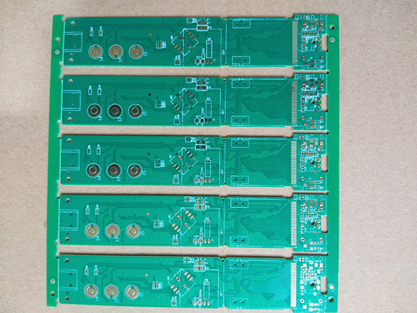
Post drilling treatment: Because the copper foil carried by the drill bit during drilling will appear on the circuit board after drilling, it is necessary to perform treatment on the circuit board after drilling. The treatment method is to directly brush the board with a brush machine to remove the oxide layer and copper wire caused by drilling on the circuit board. This step is very important. If the oxide layer is not cleaned, it will greatly reduce the adhesion of the solder mask during screen printing, leading to solder mask detachment. If the copper wire is treated cleanly during screen printing and solder mask, it may cause the copper wire to remain on the circuit board, and if the surface is not well marked, it may puncture the screen.
The final treatment of blind buried hole circuit board surface: The final treatment of the circuit board depends on what treatment the circuit board pads have undergone. If it is treated with rosin, the surface treatment should be cleaned before the pad treatment and then coated with rosin by rolling. If it is tin spraying treatment, the circuit board should be tin sprayed first and then cleaned on the surface by a brush machine. If it is an anti-oxidation treatment, the treatment method is similar to that of rolling coated rosin. The final treatment of blind buried hole circuit boards is also very important. If the treatment is not done well, residues will be left on the solder pads of the circuit board, resulting in virtual soldering or poor soldering during the soldering process.
With the rapid development of the information technology industry, some electronic products such as mobile phones and computers cannot do without the use of blind buried circuit boards. Its use is very extensive. Although blind buried circuit boards are small and inconspicuous, they can play a crucial role.
Article sourced from Jiangmen single and double-sided circuit boardhttp://www.yonghongpcb.com
-
09-09
Schematic diagram of Jiangmen single and double-sided circuit board
1. There are now various specialized PCB drawing software, such as Protel, which can draw multi-layer (including double-sided) circuit board diagrams. The layers are aligned in orientation and have vi
-
09-09
Schematic diagram of Jiangmen single and double-sided circuit board
1. There are now various specialized PCB drawing software, such as Protel, which can draw multi-layer (including double-sided) circuit board diagrams. The layers are aligned in orientation and have vi
-
09-09
Schematic diagram of Jiangmen single and double-sided circuit board
1. There are now various specialized PCB drawing software, such as Protel, which can draw multi-layer (including double-sided) circuit board diagrams. The layers are aligned in orientation and have vi
-
04-27
What is the structure of blind buried hole circuit board?
blind and buried viascircuit boardIt has the ability to freely bend, fold, and roll, and can move and stretch freely in three-dimensional space; Good heat dissipation performance and high precision; T