

How is the high-frequency four layer PCB circuit board processed?
high frequency pcb boardWiring rules
1. Rules for component placement
1). Under normal conditions, all components should be placed on the same side of the printed circuit. Only when the top layer components are too dense, can some devices with limited height and low heat generation, such as chip resistors, chip capacitors, and chip ICs, be placed on the bottom layer.
2). On the premise of ensuring electrical performance, components should be placed on a grid and parallel or straight to each other for neatness and aesthetics. In general, component stacking is not allowed; The placement of components should be compact, and input and output components should be kept as far away as possible.
3). There may be a high potential difference between certain components or wires, and their spacing should be increased to avoid accidental short circuits caused by discharge or breakdown.
4). Components with high voltage should be placed in areas that are not easily accessible by hand during debugging.
5). The components located at the edge of the board should be spaced at least 2 board thicknesses away from the edge of the board
6). The components should be evenly distributed and evenly spaced throughout the entire board surface.
2. Layout guidelines based on signal direction
1). Generally, the positions of each functional circuit unit are organized one by one according to the signal flow, with the central component of each functional circuit as the center and arranged around it.
2). The layout of components should facilitate signal flow and maintain a common direction as much as possible. In most cases, the flow of signals is organized from left to right or top to bottom, and components directly connected to the input and output terminals should be placed near the input and output connectors or connectors.
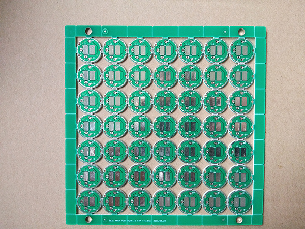
3. Avoid electromagnetic interference
1). For components with strong electromagnetic field radiation and active electromagnetic induction, the spacing between them should be increased or shielded, and the direction of component placement should intersect with adjacent printed conductors.
2). Try to avoid mixing high and low voltage devices with each other, and interlocking devices with strong and weak signals.
3). Regarding components that generate magnetic fields, such as transformers, speakers, inductors, etc., attention should be paid to reducing the cutting of magnetic lines on printed conductors during layout. The magnetic field directions of adjacent components should be straight to each other to reduce coupling between them.
4). Shield the disturbance source, and the shielding cover should have excellent grounding.
5). In circuits operating at high frequencies, the influence of distributed parameters between components should be considered.
4. Suppress thermal disturbance
1). Regarding heating elements, priority should be given to organizing them in locations that are conducive to heat dissipation. If necessary, a separate radiator or small fan can be set up to reduce temperature and minimize the impact on adjacent elements.
2). Some high-power integrated blocks, large or medium power transistors, resistors, and other components should be placed in areas that are easy to dissipate heat and separated from other components.
3). Thermistors should be tightly attached to the tested component and kept away from high-temperature areas to avoid being affected by other heat generating equivalent components and causing misoperation.
4). When placing components on both sides, heating elements are generally not placed on the bottom layer.
5. Layout of adjustable components
The layout of adjustable components such as potentiometers, variable capacitors, adjustable inductance coils, or micro switches should consider the structural requirements of the entire machine. If they are adjusted outside the machine, their positions should be adapted to the position of the adjustment knob on the chassis panel; If it is for in machine conditioning, it should be placed on the printed circuit board at the conditioning location.
Article sourced from Jiangmen single and double-sided circuit boardhttp://www.yonghongpcb.com
-
09-09
Schematic diagram of Jiangmen single and double-sided circuit board
1. There are now various specialized PCB drawing software, such as Protel, which can draw multi-layer (including double-sided) circuit board diagrams. The layers are aligned in orientation and have vi
-
09-09
Schematic diagram of Jiangmen single and double-sided circuit board
1. There are now various specialized PCB drawing software, such as Protel, which can draw multi-layer (including double-sided) circuit board diagrams. The layers are aligned in orientation and have vi
-
09-09
Schematic diagram of Jiangmen single and double-sided circuit board
1. There are now various specialized PCB drawing software, such as Protel, which can draw multi-layer (including double-sided) circuit board diagrams. The layers are aligned in orientation and have vi
-
04-27
What is the structure of blind buried hole circuit board?
blind and buried viascircuit boardIt has the ability to freely bend, fold, and roll, and can move and stretch freely in three-dimensional space; Good heat dissipation performance and high precision; T