

Production process of circuit board production
The copper foil substrate is first cut into sizes suitable for processing and production. Before laminating the substrate, it is usually necessary to roughen the copper foil on the surface of the board using methods such as brushing, grinding, and micro etching, and then attach the dry film photoresist to it with appropriate temperature and pressure. Send the substrate with the dry film photoresist attached to it into a UV exposure machine for exposure. The photoresist will undergo polymerization reaction in the transparent area of the film when exposed to UV light, and the circuit impressions on the film will be transferred to the surface of the dry film photoresist. After tearing off the maintenance adhesive film on the film surface, first use sodium carbonate aqueous solution to develop and remove the areas on the film surface that have not been exposed to light, and then use a mixed solution of hydrogen peroxide to corrode and remove the exposed copper foil, forming a circuit. Finally, the dry film that has been successfully removed will be washed away using a light oxidizing aqueous solution.
After lamination, the inner circuit board must be bonded to the outer circuit copper foil with glass fiber resin film. Before lamination, the inner layer board needs to undergo blackening (oxygenation) treatment to passivate the copper surface and add insulation properties; And roughen the copper surface of the inner layer circuit to ensure good adhesion performance with the film. When stacking, first use a riveting machine to rivet the inner layer circuit boards with six or more layers of circuits in pairs. Then neatly stack them on top of the mirror steel plates using a tray, and send them into a vacuum laminating machine to harden and bond the film at an appropriate temperature and pressure. The pressed circuit board uses an X-ray active positioning drilling target machine to drill target holes as reference holes for aligning the inner and outer circuits. And cut the edges of the board appropriately to facilitate subsequent processing
[Drilling] Use a CNC drilling machine to drill the conductive holes for interlayer circuits and the fixing holes for welded parts on the circuit board. When drilling, use a plug to fix the circuit board to the drilling machine table through the previously drilled target hole, and add a flat lower pad (phenolic resin board or wood pulp board) and upper cover plate (aluminum plate) to reduce the occurrence of drilling burrs
After the formation of interlayer conductive channels, a metal copper layer needs to be laid on them to complete the conduction of interlayer circuits. First, use heavy brushing and high-pressure washing to clean the hair on the hole and the powder particles in the hole. Soak and attach tin to the cleaned hole wall
Once copper is deposited on the palladium gel layer, it is then reduced to metallic palladium. Immerse the circuit board in a chemical copper solution, and use the catalytic effect of palladium metal to reduce and deposit copper ions in the solution onto the pore walls, forming a through-hole circuit. Then, the copper layer inside the via hole is thickened to a thickness that can resist subsequent processing and environmental impacts using copper sulfate bath electroplating.
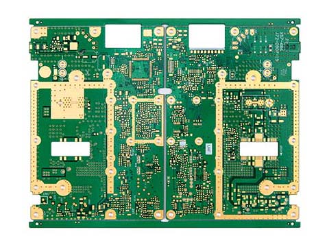
The secondary copper of the outer layer circuit is similar to the inner layer circuit in the manufacturing of circuit impression handling, but there are two production methods for circuit etching: positive and negative films. The production method of negative film is similar to that of inner layer circuit manufacturing, which is completed by directly etching copper and removing the film after development. The production method of positive film is to add secondary copper and tin lead plating after development (the tin lead in this area will be preserved as an etching inhibitor in the later copper etching step), remove the film, and use a mixture of alkaline ammonia water and copper chloride solution to corrode and remove the exposed copper foil, forming a circuit. Finally, the tin lead stripping solution is used to strip off the retired tin lead layer (there was a practice in the early stages of preserving the tin lead layer, which was remelted and used to wrap the circuit as a maintenance layer, but now it is mostly unnecessary).
Anti welding ink text printing: In the early stages, green paint was produced by directly heating (or UV irradiation) the film after screen printing to harden it. However, due to the frequent infiltration of green paint into the copper surface of the circuit terminal contacts during printing and hardening, there are difficulties in soldering and using the parts. Nowadays, in addition to the use of rough and simple circuit boards, photosensitive green paint is often used for production.
Print the text, trademark, or part number required by the customer onto the board using screen printing, and then cure the text ink by hot drying (or UV irradiation).
【 Contact Processing 】 Anti welding green paint covers most of the copper surface of the circuit, only revealing the terminal contacts for component welding, electrical testing, and circuit board insertion. This endpoint needs to be properly maintained to prevent oxidation at the endpoint connected to the anode ( ) during long-term use, which may affect circuit stability and pose safety concerns.
Cut the circuit board into the required external dimensions using a CNC molding machine (or mold punch). When cutting, use a plug to fix the circuit board onto the bed (or mold) through the positioning hole drilled from the front for molding. Cut open the golden finger area and then perform oblique grinding to facilitate the insertion and use of the circuit board. For multi chip formed circuit boards, it is often necessary to add X-shaped break wires to facilitate customers' disassembly and splitting after insertion. Finally, clean the powder and surface ion pollutants on the circuit board.
Common packaging: PE film packaging, heat shrink film packaging, vacuum packaging, etc
Article source: PCB manufacturerhttp://www.yonghongpcb.com/
-
09-09
Schematic diagram of Jiangmen single and double-sided circuit board
1. There are now various specialized PCB drawing software, such as Protel, which can draw multi-layer (including double-sided) circuit board diagrams. The layers are aligned in orientation and have vi
-
09-09
Schematic diagram of Jiangmen single and double-sided circuit board
1. There are now various specialized PCB drawing software, such as Protel, which can draw multi-layer (including double-sided) circuit board diagrams. The layers are aligned in orientation and have vi
-
09-09
Schematic diagram of Jiangmen single and double-sided circuit board
1. There are now various specialized PCB drawing software, such as Protel, which can draw multi-layer (including double-sided) circuit board diagrams. The layers are aligned in orientation and have vi
-
04-27
What is the structure of blind buried hole circuit board?
blind and buried viascircuit boardIt has the ability to freely bend, fold, and roll, and can move and stretch freely in three-dimensional space; Good heat dissipation performance and high precision; T