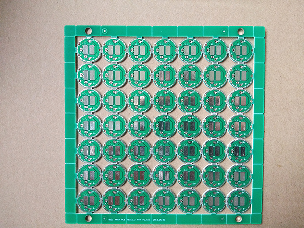
How are the high frequency four-layer PCB circuit boards processed?
High Frequency PCB Board Wiring rules
1. Component placement rules
1).Under general conditions, all components should be placed on the same surface of the printed circuit. Only when the top components are too dense, can some devices with limited height and low calorific value, such as patch resistance, patch capacitance, and patch IC, be placed on the bottom.
2).On the premise of guaranteeing the electrical performance, the components should be placed on the grids and parallel or straight to each other in order to be regular and beautiful. In general, stacking of components is not allowed; the components should be placed compactly, and the input and output components should be as far away as possible.
3).There may be a high potential difference between some components or wires, so their spacing should be increased to avoid accidental short circuit caused by discharge and breakdown.
4).Components with high voltage should be placed as far as possible in places that are not easily touched by hands during commissioning.
5).Components sitting at the edge of the Board shall be at least two plate thicknesses apart from the edge of the board.
6).Components should be distributed evenly and densely on the whole plate surface.
2. Layout criteria according to signal orientation
1).Generally, according to the signal flow, each functional circuit unit is organized one by one, and the central component of each functional circuit is taken as the center, and the layout is carried out around it.
2).The layout of components should facilitate the flow of signals and keep them in the same direction as possible. In most cases, the flow direction of the signal is organized from left to right or from top to bottom. The components directly connected to the input and output terminals should be placed near the input and output connectors or connectors.

3. Avoid electromagnetic disturbance
1).For the components with strong radiation electromagnetic field and active electromagnetic induction, the interval between them should be increased or shielded. The direction of the components should be intersected with the adjacent printed guidance lines.
2).Avoid mixing high and low voltage devices with each other and interlacing strong and weak signal devices as far as possible.
3).As for the components that can generate magnetic field, such as transformers, loudspeakers, inductors, etc., attention should be paid to reducing the cutting of magnetic lines to printed guidance lines when they are laid out. The magnetic field directions of adjacent components should be straight with each other, so as to reduce the coupling between them.
4).Shielding the disturbing source, the shielding cover should have outstanding grounding.
5).In high-frequency circuit, the influence of distribution parameters between components should be considered.
4. Suppression of thermal disturbance
1).Regarding heating elements, priority should be given to locating in a position conducive to heat dissipation. If necessary, a radiator or a small fan can be set alone to reduce temperature and influence on adjacent elements.
2).Some high-power integrated blocks, large or medium-power transistors, resistors and other components should be placed in places where heat dissipation is easy, and separated from other components.
3).Thermistors should be close to the tested components and far away from the high temperature area, so as to avoid the influence of other heating power equivalent components and cause misoperation.
4).When double-sided elements are placed, the heating elements are generally not placed in the bottom layer.
5. Layout of adjustable components
The layout of adjustable elements such as potentiometers, variable capacitors, adjustable inductance coils or micro-switches should take into account the structural requirements of the whole machine. If the machine is conditioned outside, its position should be suitable for the position of the conditioning knob on the box panel; if the machine is conditioned inside, the printed circuit board should be placed in the conditioning area.
The article originates from Jiangmen Single-sided and Double-sided Circuit Board http://www.yonghongpcb.com
-
07-18
What is the structure of blind buried hole circuit board?
Blind buried-hole circuit boards have the characteristics of free zigzag, folding and winding, free movement and expansion in three-dimensional space, good heat dissipation performance and high precis
-
07-18
What role does copper play in circuit boards?
PCB manufacturers take you to know that there are several reasons for PCB copper laying: 1. EMC can shield large area of ground or power supply copper, and some special areas, such as PGND, play a pr
-
07-18
Four matters needing attention in choosing PCB manufacturer
When choosing PCB manufacturers, the price of PCB manufactured by professional manufacturers will be more affordable, and the quality assurance will be stronger, which will be more guaranteed after
-
07-18
How to use three glue-proof PCB correctly?
Sanfang gum does not contain evaporative substances such as acetone and xylene, which is more environmentally friendly and safe. Mainly used in electronic circuits and components to form a protectiv